
 Tweet
Tweet
Originally posted by coder
View Post
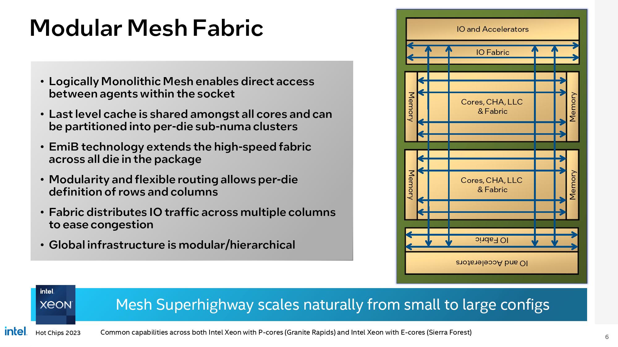
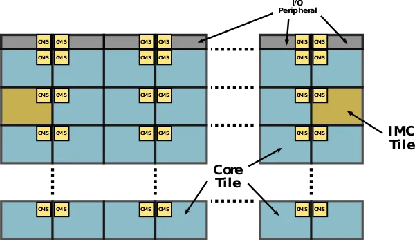
The fact that Granite Rapids has I/O dies for OFF CHIP COMMUNICATION proves the point I was making and shows that you don't understand what "glue" actually means. Of course Granite Rapids has I/O -- duh -- but those I/O dies are used exclusively for communicating OFF PACKAGE. with other components in the system. To say that any chip that has I/O capabilities is "glued together" shows you don't understand the meaning of the term.
And yes, of course there are ways for different cores to talk to each other in Granite Rapid -- once again, duh -- but the mesh network is NOT re-encoding every piece of data into a quasi-PCIe packet protocol and shoving it through a SERDES to another transceiver just to move some bits between L3 slices. Note that those I/O chiplets are NOT placed between every single compute tile because they aren't necessary, they are only used to communicate off-package with your GPUs, disks, networking, etc. etc.
I will admit that I was not wrong but incomplete on one point: There IS glue on Granite Rapids... for communicating with other sockets in a multi-socket system. That's what the UPI links are and UPI is basically what AMD copied (UPI was around for years prior to Zen) as "Infinity Fabric" for its chiplets. So there is glue for multi-socket systems, and if you actually understand what glue means you'd know that every Zen system is basically a large multi-socket setup on a logical level even if the dies are physically placed in single sockets.
Comment