Announcement

Collapse
No announcement yet.

AVX / AVX2 / AVX-512 Performance + Power On Intel Rocket Lake

Collapse
X
 
  • Filter
  • Time
  • Show
Clear All
new posts

  • #41
    Originally posted by coder View Post
    No, they made plenty of general-purpose improvements in both Sunny Cove and Willow Cove. We probably don't see it so much on Rocket Lake, because it's a backport to 14 nm. Anandtech confirmed IPC increases in both Ice Lake (laptop) and Tiger Lake, though the latter still has slightly lower IPC than Zen3.
    Actually Willow Cove didn't see much of any IPC gains. Tiger Lake is only faster than Ice Lake in general because it had much higher clock frequencies.

    Ice Lake did see significant IPC gains vs the old Skylake architecture, and it's essentially the same chip as what ended up in Rocket Lake and Tiger Lake. They just updated the manufacturing processes to clock faster, and the latter has an updated cache design.

    Originally posted by anandtech
    IPC improvements of Willow Cove are quite mixed. In some rare workloads which can fully take advantage of the cache increases we’re seeing 9-10% improvements, but these are more of an exception rather than the rule. In other workloads we saw some quite odd performance regressions, especially in tests with high memory pressure where the design saw ~5-12% regressions. As a geometric mean across all the SPEC workloads and normalised for frequency, Tiger Lake showed 97% of the performance per clock of Ice Lake.
    Last edited by smitty3268; 08 April 2021, 10:58 AM.

    Comment


    • #42
      Originally posted by coder View Post
      Ugh. Why do people try to decide for themselves what he doesn't like about it? Is it really that hard to google "torvalds AVX-512" and find his actual statement?
      I did read his comments on that thread and he nowhere expresses a concern for the implementation of AVX-512, but instead, laments the idea of adding specialized instruction sets like it for maginal use. Instead, like most of us, he would prefer to see those resources (both design and silicon) go into making normal integer workloads run faster.

      Comment


      • #43
        After seeing the graphs in the article, I think what we need is a power-optimized AVX-512 implementation. The instruction set is powerful and the problems with it come from how it is executed by the hardware. Using less power would result in lower performance but should still be faster than AVX 2.

        You could do this by making 512-bit instructions take extra cycles to execute, spreading the energy over a longer period of time to reduce power. With more forgiving instruction timing, slower but more power-efficient digital logic circuits could be chosen, further reducing power.

        Comment


        • #44
          Originally posted by foobaz View Post
          After seeing the graphs in the article, I think what we need is a power-optimized AVX-512 implementation.
          With just one AVX512 vector unit (or 2x256 joining to make 1x512) it's going to be as power-optimized as it gets. Given the process node that is (14nm)... which is power hungry.

          The problem is that with 1x512 instead of 2x512 vector units we are not getting double the performance, as the server and HEDT chips get. Thus we get high energy draw and not much benefit in terms of performance.

          Now regarding power per se, I think this will be solved somewhat as chip size goes down at 10 and then 7nm. Most of the press will be quick to point out big power draws as vector size doubles but in the end of the day what counts is how much performance you extract per watt. How can you extract more perf per watt? You go wider but clock the vector unit lower and with a lower voltage draw. Thus if you were to gain 2x in performance (flops) by going 2x wider at the same speeds, you get the clocks down like 20-30%, and you are still 1.4x - 1.6x up in performance and maybe at a much better perf per watt compared to full-speed AVX2 units. Wider and slower is the way to increase perf/watt almost everywhere.

          The problem then becomes what to do with the underclocking when the occasional avx512 instruction comes up. Maybe the chip shouldn't even underclock if this happens for just a while and thus maintain full speed. Maybe it should start underclocking when real heavy avx512 utilization comes into place, not triggered by a few instructions or so. Or maybe the entire cpu architecture could get a serious IPC upgrade like 30-40% to keep clocks low and uniform among the vector and scalar unit, a la M1. It's doable but x86 improvements have been stalling for so long that even mobile chips went ahead in terms of IPC.

          Comment


          • #45
            Originally posted by smitty3268 View Post
            Actually Willow Cove didn't see much of any IPC gains. Tiger Lake is only faster than Ice Lake in general because it had much higher clock frequencies.
            Okay, my bad.

            They did go nuts on the caches, though. L2 is 2.5x the size of Ice Lake's, with 20-way associativity instead of 8-way, and now non-inclusive. L3 got boosted by 1.5x, but actually lost a little associativity (16-way to 12-way) and is also now non-inclusive.

            Increasing cache sizes is like trying to gin up performance by just throwing transistors at the problem. It's not the cheapest or necessarily the most power-efficient way to improve performance, but it's nearly always good for at least a couple %.

            It tickles me to think that you could now fit the entire address range of an original PC in the L2 cache of one core!

            Originally posted by smitty3268 View Post
            Ice Lake did see significant IPC gains vs the old Skylake architecture, and it's essentially the same chip as what ended up in Rocket Lake and Tiger Lake. They just updated the manufacturing processes to clock faster, and the latter has an updated cache design.
            Did anyone actually validate that Rocket Lake delivers the same IPC as Ice Lake? Because it's not hard to imagine some latency or pipeline stages had to be added to make that uArch (originally designed for 10 nm) work at 14 nm.

            Comment


            • #46
              Originally posted by foobaz View Post
              After seeing the graphs in the article, I think what we need is a power-optimized AVX-512 implementation.
              That's exactly what Skylake SP and Cascade Lake SP did, and it's why their clock-throttling was so horrendous. Server CPUs are pretty strict about staying within their power envelope.

              Originally posted by foobaz View Post
              Using less power would result in lower performance but should still be faster than AVX 2.
              ...unless you're using enough AVX-512 to trigger clock-throttling, but not enough to deliver a big speedup. The net-result is a workload-wide slowdown that can be quite dramatic.

              For a good case study, see: https://blog.cloudflare.com/on-the-d...uency-scaling/

              Originally posted by foobaz View Post
              You could do this by making 512-bit instructions take extra cycles to execute, spreading the energy over a longer period of time to reduce power. With more forgiving instruction timing, slower but more power-efficient digital logic circuits could be chosen, further reducing power.
              Their CPU cores don't have a separate clock domain for AVX-512, which could increase latency and add other complications. And if you went straight to halving the throughput of AVX-512, then it would lose most of its benefits over AVX2.

              Basically, Intel pushed AVX-512 before the manufacturing tech was ready for it. If they'd waited to deploy it on 10 nm, then it wouldn't be so bad. It still causes clock throttling in Ice Lake SP*, but probably more like the situation we had with AVX2 on Haswell, where I don't think anyone actually talked about it actually being a liability.

              * Note: I have yet to see good data on this, so I'm basically taking Intel at their word that they've addressed the main issues.

              Comment


              • #47
                Originally posted by _Alex_ View Post
                The problem then becomes what to do with the underclocking when the occasional avx512 instruction comes up. Maybe the chip shouldn't even underclock if this happens for just a while and thus maintain full speed. Maybe it should start underclocking when real heavy avx512 utilization comes into place, not triggered by a few instructions or so.
                There's some critical instruction density that triggers the down-clock, and I think there are at least 2 tiers of throttling. The problem seems to be that Skylake SP and Cascade Lake throttle down a lot more readily than they restore clocks back up. Changing clock frequency does have some overheads, so I can understand why they are a little lazy about it, otherwise it could potentially eat up as much performance as you'd regain from running at a higher frequency for a little while.

                Originally posted by _Alex_ View Post
                Or maybe the entire cpu architecture could get a serious IPC upgrade like 30-40% to keep clocks low and uniform among the vector and scalar unit, a la M1. It's doable but x86 improvements have been stalling for so long that even mobile chips went ahead in terms of IPC.
                You touch on a good point, which is that this is one of the problems you run into, by trying to use a high-clocking, general-purpose CPU core to compete with low-clocking GPUs. GPUs are slow and wide for a reason -- because that's the best way to scale up performance. Intel seems to have missed that, when they thought they could just bolt-on AVX-512 to their 14 nm CPUs.

                I think it's notable that Apple bypassed SVE, in their M1. However, since the SoC also has a dedicated NPU, ISP, and GPU, there wouldn't be much left for it to actually do. As for equaling the M1's IPC, this is complicated by the x86 ISA.

                The only non-Intel example I know of, where a general-purpose CPU implemented 512-bit vector operations is Fujitsu's A64FX. It's both made on TSMC 7 nm and clocks only up to 2.2 GHz (or just 1.8 GHz, in HPE's air-cooled chassis that's available to the general public). But, it also has 48 of those cores. So, it's further confirmation that wide-and-slow is the way to go.

                Intel really failed to think through the implications of their AVX-512 strategy. AMD did well to stand back from that train wreck.

                Comment


                • #48
                  Bottom line:
                  1. According to results AVX may safely be thrown out of modern consumer CPUs. It does not give much and the chip space it takes can be utilized for other purposes. L1 cache and/or additional general purpose registers looking the most prominent of such.
                  2. 'Best of both worlds' case is sitting down with just base AVX or worst case AVX-256.
                  3. AVX-512 is too niche, wastes power in most tasks and also wasting the chip space/thermal budget available.

                  P.S. For very niche tasks benefitting of it, external accelerators like GPUs look more viable than just having it in the main CPU.
                  Last edited by Alex/AT; 09 April 2021, 01:56 AM.

                  Comment


                  • #49
                    Originally posted by Alex/AT View Post
                    Bottom line:
                    1. According to results AVX may safely be thrown out of modern consumer CPUs. It does not give much and the chip space it takes can be utilized for other purposes. L1 cache and/or additional general purpose registers looking the most prominent of such.
                    2. 'Best of both worlds' case is sitting down with just base AVX or worst case AVX-256.
                    3. AVX-512 is too niche, wastes power in most tasks and also wasting the chip space/thermal budget available.

                    P.S. For very niche tasks benefitting of it, external accelerators like GPUs look more viable than just having it in the main CPU.
                    This pretty much sums it up. Of course Intel can't have that because -at the moment- they don't sell GPUs.

                    Comment


                    • #50
                      Originally posted by TemplarGR View Post
                      This pretty much sums it up. Of course Intel can't have that because -at the moment- they don't sell GPUs.
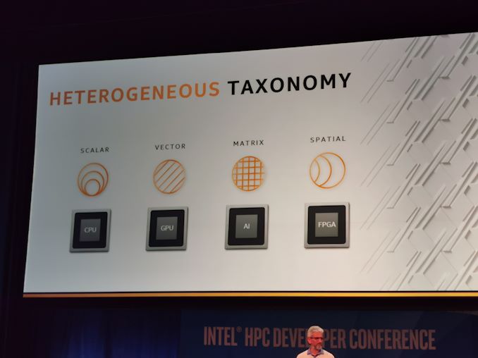
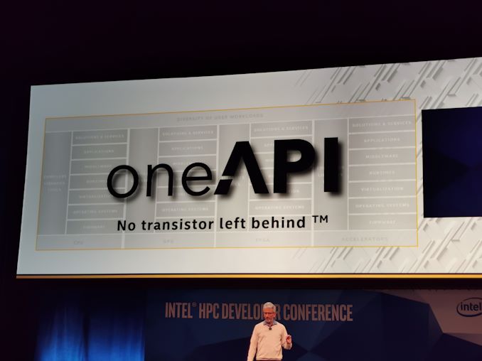
                      Their stated strategy is to offer some level of capability on all devices, from CPU -> GPU -> FPGA -> AI processors. That's what oneAPI is all about.


                      Of course, some of that is probably working backwards from the situation they got into by trying to use their x86 CPUs as the singular hammer to attack all compute problems.


                      If we didn't know any better, that wouldn't sound like a bad approach.

                      Source: https://www.anandtech.com/show/15123...pm-mt-11pm-utc

                      Comment

                      Working...
                      X