
 Tweet
Tweet
Originally posted by Dukenukemx
View Post
just go back to th e moment all chips where 2D chips it was on AMD side 34nm SOI node and intels 45nm node.
"this is the first I've ever heard this."
well not many people are sooooooo deep in this topic.
and i am a person who do not copy other people what means talking with me is unique.
at 45nm intel discovered that the price to make the transistors smaller goes up very fast and to the point that the node becomes to expensive for any product. then they did go a different direction.
similar to 100gb BDXL blue ray discs they did start to use multible layers it is like the 3D stacking of the 5800X3D but they do not stack these final chips instead they make the die in a way that tranistor is over another tranistor in 3D.
as you know at the time of AMD bulldozer with 34nm intel could easily beat AMD because they managed to make their 45nm node look like a 22/28nm node if you see it in the meaning of density in 2D
intel hat 2 problems: higher real nm node means less clock speed and also bigger tranistors means more heat.
but they did fix both with ISA war and plain and simple bigger chips with more tranistors and lower-clock speed.
remember an bulldozer on 34nm in OC could easily beat any intel cpu in clock speed.
Originally posted by Dukenukemx
View Post
today all do it in the same way: they count the amount of transistors on 1mm² and then they calculate it like it is a 2D node.... this means IBM 2nm node has the density of a 2nm 2D node but because it is 3D design nothing of this node under a microscope will have any size of 2nm...
Originally posted by Dukenukemx
View Post
Dark silicon is such a big problem with these modern notes that these companies need to produce and sell these products of these nodes longer just to make sure the high costs will come in again from the sales.
for example apple did drop 3nm/4nm for iphone chips because the costs are so high the price of a smartphone would go out of control...
i found links for you:
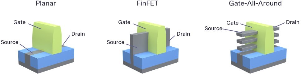
" Intel reinvents transistors using new 3-D structure for 22 nanometer chips"
this is an article from 2011 it is the history in how intel did defeat AMD
in the mening of 2D planar transistors AMD had the better node but intel did manage to make their inferior 45nm node look like it is a 22/28nm node.
and nother article about building tranistors on wavers in 3D to get more density
file:///home/q/Downloads/applsci-07-01047.pdf
this is an PDF about do CMOS tranistors going from 2D to 3D to get maximum of density


Comment