Announcement

Collapse
No announcement yet.

NVIDIA Announces Grace CPU For ARM-Based AI/HPC Processor

Collapse
X
 
  • Filter
  • Time
  • Show
Clear All
new posts

  • #91
    Originally posted by Jumbotron View Post
    What that will entail is that even your Linux desktop of the future much less your smartphone and Chromebook will have the power of the ENTIRE data center at your disposal with latencies that rival some board connected to a PCIe slot.
    This is physically impossible. You can get latencies down to a point, but you can't change the speed of light or realistically put mini datacenters within a few miles of everyone.

    Originally posted by Jumbotron View Post
    Intel saw the future and never really put the GPU on the die, they put their shitty GPUs in the package. Instead of SoC, it was SiP. System in a Package.
    That's mostly untrue. With a handful of exceptions, Intel did put them on-die. You can find die shots of pretty much every Intel desktop CPU where someone has marked out the floorplan and estimated the area of the CPU cores, GPU, L3 cache, etc.

    Originally posted by Jumbotron View Post
    AMD has gone whole hog "chiplets". It's starting to look like the entire CPU package is the size of an entire Raspberry Pi.
    Again, this flies in the face of simple facts. AM4 is "standard" sized. More notably, even their latest APUs use a monolithic die, which suggests some real limitations of the chiplet approach. If chiplets were a viable option, one would think they could've saved a lot of time and money by reusing the CPU die from Ryzen 5000 desktop processors and just pairing it with a GPU and I/O die. Yet, in spite of all their chiplet experience, every APU they've done has been monolithic, which is a very strong testament to either its superior energy efficiency or the production cost advantages at that size and below.

    Originally posted by Jumbotron View Post
    Pretty soon, you won't have room for slots. Because the entire motherboard WILL BE THE SiP.
    Intel most recently went to a 1200-contact package, which is a far cry from dinner plate-sized packages. We've yet to see what AMD's next mainstream socket looks like, but I expect it won't be much bigger than it is now.

    I can even see scenarios where server CPU packages could end up with fewer pins.

    Originally posted by Jumbotron View Post
    Think smartphones with computational photographic elements where the compute DSP or NPU is at the lens itself and NOT on a DPS or NPU in the SoC.
    No, that's silly. I can see potential benefits from putting a limited amount of compute in the sensor, but not a full-blown NPU.

    Originally posted by Jumbotron View Post
    2: Increasingly OFF board and OFF device. Streaming game services such as Stadia and GeForce Now point the way.
    Game streaming has been around for over a decade and I have yet to see consoles cease production. We'll just see how far it goes.

    Originally posted by Jumbotron View Post
    when's the last time you even plugged in a modem card at all? It's all on the motherboard now.
    I still use a modem, but it's external and broadband. The main reason is because it's easier to share with other devices, that way.

    Originally posted by Jumbotron View Post
    Sound card anyone? 98% of the world doesn't even know they STILL make sound cards.
    Musicians do.

    Originally posted by Jumbotron View Post
    What about Firewire?
    This is silly. You can list a dozen obsolete standards, but there are still RAID cards, high-speed & multi-port NICs, Thunderbolt, USB 3.2, SATA, M.2 carriers, FPGA boards, multi-track audio, and dozens of industrial uses. There are still half-height, half-length PCIe SSDs for enterprise, like I have in my workstation. Last, but not least, dGPUs and AI accelerator cards.

    Ask AI researchers and they will tell you that if you need to do lots of training of models that can fit on a few PC GPUs, then it's still much more cost-effective to buy your own than use GPUs in the cloud.

    Originally posted by Jumbotron View Post
    Consolidation, integration, miniaturization. That is how we now have the prevailing compute paradigm which has driven "Desktop" sales into the gutter.
    Except they're not. Desktop has had a major resurgence, in the past several years! It will continue to be a force, in computing, much longer than you think.

    Originally posted by Jumbotron View Post
    And all those platforms have either as standard equipment or as an option upon ordering, cellular capability.
    Uh, no. I have like a dozen devices in my home that need internet. There's no way I'm paying for 5G connectivity for each. I explicitly use wi fi on my phone, to avoid data charges for going over cell and because the quality of voice calls is better. And even 4G cell coverage isn't great, in a lot of places. I live just outside a major city and only get 1-2 bars of signal strength on my phone.

    Conversely, my land-based internet connection is fast and stable.

    I think I get your main issue, though. You see trends and overestimate their speed and sweep. That's why you think desktops, consoles, and land-based internet will soon cease to exist, and why you think ARM already dominates everything. The problem is that you ignore everything that doesn't fit your nice narrative, like Chinese SoCs and GPUs. Also, I'd worry you'd switch sides, in a war where your side suffered a few early losses.

    I think it's much more interesting to try and pierce through the hype, than to get swept up in it. To me, what makes trends interesting is to not only to think about their implications, but also where and why they could break down. I used to think ARM would be way more dominant than it is, by now. I think there are lessons in that, if one is willing to look beneath the surface.

    Comment


    • #92
      Originally posted by coder View Post
      Again, this flies in the face of simple facts. AM4 is "standard" sized. More notably, even their latest APUs use a monolithic die, which suggests some real limitations of the chiplet approach. If chiplets were a viable option, one would think they could've saved a lot of time and money by reusing the CPU die from Ryzen 5000 desktop processors and just pairing it with a GPU and I/O die. Yet, in spite of all their chiplet experience, every APU they've done has been monolithic, which is a very strong testament to either its superior energy efficiency or the production cost advantages at that size and below.
      The AMD APU actions does not say chiplets were not a valid option. Key note Ryzen 5000 APU the GPU part is a Vega 8. That the same GPU as the 2000 series Ryzen APUs. Yes the first Ryzen APUs. Most people have not noticed that every Ryzen APU is the same GPU just made at different nm of course improved nm has given some improved performance.

      coder the reality here is so far AMD has not major revised the APU GPU so far.


      There is very interesting patent that AMD has taken out for rdna2/3. Does not mean they are going to do it. But patent documents a cpu with IO dia with multiable GPU chiplets in a single package. Also documents using the same chip-lets to build discrete graphics cards.

      Yes this patent is when AMD is finally looking at redoing the APU GPU. Reality here AMD has not need redo the AMD APU GPU because Intel igpu offerings were not that competitive and that has recently changed.

      The reason why APU of AMD has been a single block is less validation and no new GPU design. A chiplet change on the GPU for APU would have increased validation cost when you were not changing the GPU design. When doing GPU design upgrade a full validation has to be done anyhow so there will be no extra cost at that point to go chiplet if it a functional design.

      Think when was the last time you saw vega inside a current generation AMD dGPU. Remember the big reason for chiplet of the cores with APU less ryzens is to share chiplets between the epyc and the lower market. For a chiplet APU to make proper sense the APU GPU needs to be on the same technology as the dGPU so they can share chiplets to reduce production cost.

      Basically it has not made sense for AMD to change their APU yet. But going forwards it could make a lot of sense to change the APU GPU to a chiplet at the same time they change the dGPU to chiplet.


      Comment


      • #93
        Originally posted by oiaohm View Post
        The AMD APU actions does not say chiplets were not a valid option.
        Yes, it absolutely does! Do you honestly think that if chiplets made sense for APU, AMD wouldn't be using them after 4 years and at 4 generations?

        Originally posted by oiaohm View Post
        Key note Ryzen 5000 APU the GPU part is a Vega 8. That the same GPU as the 2000 series Ryzen APUs.
        That has nothing to do with anything! If chiplets made sense for APUs, they could've much more easily made a vega8 chiplet than to keep porting that block to each new APU die!

        Originally posted by oiaohm View Post
        Most people have not noticed that every Ryzen APU is the same GPU just made at different nm of course improved nm has given some improved performance.

        coder the reality here is so far AMD has not major revised the APU GPU so far.
        Factually inaccurate. AMD made other changes to the GPU block, to squeeze more performance from it.


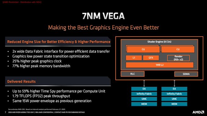
        On the GPU side is where we see bigger changes. AMD does two significant things here – it has reduced the maximum number of graphics compute units from 11 to 8, but also claims a +59% improvement in graphics performance per compute unit despite using the same Vega graphics architecture as in the prior generation. Overall, AMD says, this affords a peak compute throughput of 1.79 TFLOPS (FP32), up from 1.41 TFLOPS (FP32) on the previous generation, or a +27% increase overall.


        AMD manages to improve the raw performance per compute unit through a number of changes to the design of the APU. Some of this is down to using 7nm, but some is down to design decisions, but it also requires a lot of work on the physical implementation side.

        For example, the 25% higher peak graphics frequency (up from 1400 MHz to 1750 MHz) comes down a lot to physical implementation of the compute units. Part of the performance uplift is also due to memory bandwidth – the new Renoir design can support LPDDR4X-4266 at 68.3 GB/s, compared to DDR4-2400 at 38.4 GB/s. Most GPU designs need more memory bandwidth, especially APUs, so this will help drastically on that front.

        There are also improvements in the data fabric. For GPUs, the data fabric is twice as wide, allowing for less overhead when bulk transferring data into the compute units. This technically increases idle power a little bit compared the previous design, however the move to 7nm easily takes that onboard. With less power overhead for bulk transfer data, this makes more power available to the GPU cores, which in turn means they can run at a higher frequency.
        Source: https://www.anandtech.com/show/15624...pu-uncovered/2

        Originally posted by oiaohm View Post
        There is very interesting patent that AMD has taken out for rdna2/3. Does not mean they are going to do it. But patent documents a cpu with IO dia with multiable GPU chiplets in a single package. Also documents using the same chip-lets to build discrete graphics cards.
        I'm not saying we'll never see an APU with chiplets. In fact, Intel has already put the GPU on a separate die, a few times. I'm just saying chiplets aren't necessarily the obvious panacea that some people claim.

        But technology improves and it wouldn't surprise me to see the threshold change for where it makes sense to use them. Particularly if defects are worse on 5 nm. In fact, even if they aren't, the higher wafer price for EUV means that even existing defect rates will become more costly.

        Originally posted by oiaohm View Post
        For a chiplet APU to make proper sense the APU GPU needs to be on the same technology as the dGPU so they can share chiplets to reduce production cost.
        That's just wrong. If a chiplet-based APU made sense, then it should be cheaper to make a die with the GPU portion that what it now costs them to integrate the GPU block with the current APU die. Especially if they're planning on reusing that chiplet for multiple APU generations.

        In fact, it's unlikely they'll use (hypothetical) dGPU chiplets in their APUs, simply because dGPUs are so much more powerful that their chiplets are going to have to be a lot bigger. And if you look at the GFLOPS/bandwidth ratio of their APUs vs their dGPUs, the APUs are already way more bandwidth-starved. So, it simply doesn't make sense for them to put a much bigger GPU block in an APU. It'd be wasted silicon.

        First: check you facts. Second: use some sense, please.

        Comment


        • #94
          Originally posted by coder View Post
          Yes, it absolutely does! Do you honestly think that if chiplets made sense for APU, AMD wouldn't be using them after 4 years and at 4 generations?
          That is ignoring something.
          Originally posted by coder View Post
          That has nothing to do with anything! If chiplets made sense for APUs, they could've much more easily made a vega8 chiplet than to keep porting that block to each new APU die!
          https://www.engadget.com/2018-01-07-...rx-vega-m.html
          Maybe you missed it there is a Vega chiplet. There is a key problem there. There is a reason why it has to be so large in the intel example.

          Originally posted by coder View Post
          Factually inaccurate. AMD made other changes to the GPU block, to squeeze more performance from it.
          Not when you go properly looking

          from https://www.anandtech.com/show/15624...pu-uncovered/2
          Part of the performance uplift is also due to memory bandwidth – the new Renoir design can support LPDDR4X-4266 at 68.3 GB/s, compared to DDR4-2400 at 38.4 GB/s. Most GPU designs need more memory bandwidth, especially APUs, so this will help drastically on that front.
          In a chiplet design this would be a alteration in the IO die part not the chiplet part. Vega is not designed to have a separate IO die.


          Originally posted by coder View Post
          In fact, it's unlikely they'll use (hypothetical) dGPU chiplets in their APUs, simply because dGPUs are so much more powerful that their chiplets are going to have to be a lot bigger. And if you look at the GFLOPS/bandwidth ratio of their APUs vs their dGPUs, the APUs are already way more bandwidth-starved. So, it simply doesn't make sense for them to put a much bigger GPU block in an APU. It'd be wasted silicon.
          Epyc is a lot more powerful than a ryzen cpu but the cpu core chiplets are the same size. There is a part that has to be a lot bigger in a Epyc vs Ryzen its the IO die. So the argument that dGPU are so much more powerful that their chiplets are going to have to be a lot bigger does not in fact.

          There is something so simple that is different.
          https://www.techarp.com/computer/amd...che-explained/
          Epyc and Ryzen Zen cores are designed to have a L3 and that is on the IO die in chiplet design to assist with bandwidth issues sharing a MMU. Vega GPU core does not have a L3 in a Vega using APU by AMD the CPU L3 is the Vega GPU L2. The part to chiplet GPU is implementing L3 that GPU have not historically had.

          The fact that Vega GPU does not support working with a L3 this means it means when it was chipleted for the intel chip it still had to basically duplicate up the functionality that should be shared in the IO die. Pushing something with only a L1 cache off to a chiplet is not going to work. Having to put a complete system L3 size L2 in a chiplet is not going to be cost effective either. Remember you cannot do a IO die without a cache on it if you want effectiveness.

          RDNA2 in AMD GPU designs is the first one that could possible be done chiplet. Its a common thing that is missed the common GPU design have are not L1/L2/L3 designs but just L1/L2. These are also a single complex design. There have not been "CPU Complex (CCX)" in GPU designs. Even Nvidia MCM has not really been designed around the Complex design.

          coder the reality to go chiplet and be cost effective the Vega design is not usable. RDNA2 starts ticking some of the boxes but not all them. RDNA3 is where we might finally see chiplet.

          Yes you can chiplet the Vega design but due to APU design using a GPU L2 overlapped with CPU L3 splitting this chiplet is very unfriendly as seen in the Intel AMD gpu combination chips.

          Coder is a really simple thing to miss that a chiplet design requires MMU and L3 on the IO die with a L1 and L2 in the chiplet. So a GPU design that does not support 3 layers of cache chiplet it is just not possible in APU.

          Before you say Vega in the IO die instead that has its own fair share of nightmares intel did look at that option. Basically new GPU design required to go chiplet. With the new design there is no reason why we could not APU sized chiplets on mass in a dGPU. Remember it will be just like Ryzen vs EPYC where the IO die increases size. Basically compute units of gpu put into complex.

          Chiplet design is not as simple to migrate to as it first appears. Yes making a CPU chiplet was way simpler than doing GPU chiplet due to the history on CPU side of sharing multi socketed CPUs with a single IO chip MMU so laying out a layout of how. Think about it with a GPU when have you ever seen a GPU MMU be a independent chip to the processing units.

          AMD has filed a patent for something that everyone knew would eventually happen: an MCM GPU Chiplet design. Spotted by LaFriteDavid over at Twitter and published on Freepatents.com, the document shows how AMD plans to build a GPU chiplet graphics card that is eerily reminiscent of its MCM based CPU designs. With NVIDIA working on […]


          Do note the diagrams of chips to waffer here. There are strict reasons why if you are going chiplet to make each of the chiplets as small as practical because this increases you per waffer yield. So a dgpu using a many chiplets where the chiplets are the same size as 1 APU chiplet absolutely makes sense.
          Last edited by oiaohm; 17 April 2021, 10:13 PM.

          Comment


          • #95
            Originally posted by oiaohm View Post
            https://www.engadget.com/2018-01-07-...rx-vega-m.html
            Maybe you missed it there is a Vega chiplet. There is a key problem there. There is a reason why it has to be so large in the intel example.
            That's not a chiplet, in the sense that we're discussing. That's a dGPU that happens to share the same base board as the CPU. The only way they're more integrated than a conventional dGPU is that they're continuously sharing power utilization data, so that some firmware can dynamically adjust the CPU and GPU clocks in order to for the total package to remain within its power budget.

            As for its size, it's a 24 CU Vega chip, made on 14 nm TSMC (which is larger than Intel's 14 nm, BTW). Vega maxed out at 64 CU. So, yeah, it's going to be big. Not sure what your point even was.

            Originally posted by oiaohm View Post
            Not when you go properly looking
            Please behave! You ignore everything I quoted about the design changes to the GPU, itself, and seizing on one detail outside of it? I already cited plenty to blow a hole in your silly argument that AMD is just carting around the same GPU block. So, drop the point and lets move on.

            Originally posted by oiaohm View Post
            Vega is not designed to have a separate IO die.
            In an APU context, that's a distinction without a difference. The APU version of Vega must have been adjusted to interface with the SoC's memory fabric.

            If they wanted to use chiplets from Zen2 and beyond, all they had to do was make a Vega chiplet that could utilize the Ryzen I/O die, or maybe make a special combined GPU/IO die that could be paired with a Zen2/3 chiplet and that'd be it.

            Originally posted by oiaohm View Post
            So the argument that dGPU are so much more powerful that their chiplets are going to have to be a lot bigger does not in fact.
            You missed the point. AMD dGPUs are now up to 80 CUs. It'd be insane to make one of those with 10 graphics/compute chiplets for a variety of reasons. The chiplets would necessarily have to be more in the range of 20 CUs, which is big (and wasteful) for an APU.

            Originally posted by oiaohm View Post
            in a Vega using APU by AMD the CPU L3 is the Vega GPU L2.
            Huh? Vega has L2. Show me where the APU Vega doesn't have L2?

            Originally posted by oiaohm View Post
            The fact that Vega GPU does not support working with a L3 this means it means when it was chipleted for the intel chip
            That wasn't a chiplet. That was a dGPU in the same package. They even interfaced via PCIe, for crying out loud!

            Originally posted by oiaohm View Post
            RDNA2 in AMD GPU designs is the first one that could possible be done chiplet.
            We don't know that. RDNA2's L1/L2 cache coherency happens in the graphics/compute die. As soon as you split that into multiple dies, you're going to have a cache coherency problem 10x as bad as Epyc. That's why it's a hard problem. The I/O die could certainly help, though. But, graphics data access patterns tend to limit scalability of that approach.

            Originally posted by oiaohm View Post
            With the new design there is no reason why we could not APU sized chiplets on mass in a dGPU.
            Yes, there is. Chiplet handling becomes more difficult and costly, the smaller they get. Also, the more communication you route through an I/O die (or any other fabric you use), the more overhead it adds, in terms of latency and energy-utilization.

            GPUs have 10x the bandwidth of CPUs and far more global data access patterns than most CPU workloads, which is why no chiplet-based GPUs exist. Whatever analogies you try to use from Epyc don't apply.

            Originally posted by oiaohm View Post
            There are strict reasons why if you are going chiplet to make each of the chiplets as small as practical because this increases you per waffer yield. So a dgpu using a many chiplets where the chiplets are the same size as 1 APU chiplet absolutely makes sense.
            That ignores the per-chiplet overheads, in cost and efficiency. What that means is that they're really trying to use fewer chiplets. I think the defect rate is a lot lower than you believe, and GPUs are very easy to bin by disabling a few CUs.

            Comment


            • #96
              Originally posted by coder View Post
              We don't know that. RDNA2's L1/L2 cache coherency happens in the graphics/compute die.
              Not quite RDNA2 has two groups of L2 that are connected two independent core sets. So there is in fact 2 independent units inside the 1 die with RDNA2 that don't in fact have cache coherency with each other. The shader 1 and the shader 2 engine. There is a nice little stall you can do if you can force work to be miss aligned on a RDNA2 were something being processed on shader 1 is need by shader2. Yes the L3 are no linked yes this forces going out to the fabric to cross from one side of the chip to the other.

              Interesting enough other than intentionally doing to wrong the fact the RDNA2 has broken cache coherency basically goes unnoticed. Kind of says a lot about GPU workloads maybe cache currency is not as important.

              Originally posted by coder View Post
              far more global data access patterns than most CPU workloads
              This has been presumed. MCM by nvidia is also finding that global data access may not be as much as presumed.

              Fun point is the first prototype GPUs in history like our modern GPUs had no cache currency at all only had output currency. This does require more focus on how workloads are assigned.

              Originally posted by coder View Post
              That ignores the per-chiplet overheads, in cost and efficiency. What that means is that they're really trying to use fewer chiplets. I think the defect rate is a lot lower than you believe, and GPUs are very easy to bin by disabling a few CUs.
              This is also ignoring what has been found with binning in the rizen/epyc. Yes its very easy to bin by disabling a few CU but if you objective is best possible performance you want as many of the best quality CU in the same unit disabling does not give you the highest yield in that department. Chiplets give you the ablity to put more quality CU into the upper models and poor quality into the lower models so not need to disable as many CU either this also increases y. Think lower clock speed parts a poor quality CU be there and work perfectly. Having a large single chip you can be in a horrible position where the chip is like 50 percent high quality CU and 50 percent low quality CU there is not enough high quality CU there to make a high quality product right. The odds of not having enough CU to make a high quality unit that you can charge the most money for gets worst the bigger the bit of silicon gets..

              Fewer chiplets equal bigger silicon area that equal less yield per silicon wafer due to the fact wafers are round. Chips the the current RDNA2 and the Nvidia MCM prototypes do ask lot of questions if our presumes have been correct. If they are not correct chiplet will be more than practical.

              Does bring a interesting question does the extra cost matter or overhead matter if the result is greater high end production that you get more money for. The yield factor is simple to overlook.

              Comment


              • #97
                Originally posted by oiaohm View Post
                Not quite RDNA2 has two groups of L2 that are connected two independent core sets. So there is in fact 2 independent units inside the 1 die with RDNA2 that don't in fact have cache coherency with each other. The shader 1 and the shader 2 engine. There is a nice little stall you can do if you can force work to be miss aligned on a RDNA2 were something being processed on shader 1 is need by shader2. Yes the L3 are no linked yes this forces going out to the fabric to cross from one side of the chip to the other.

                Interesting enough other than intentionally doing to wrong the fact the RDNA2 has broken cache coherency basically goes unnoticed. Kind of says a lot about GPU workloads maybe cache currency is not as important.
                Cite references, please. I think you are confusing directly-addressed, local memory with cache. Some modern GPUs can switch the behavior of (some) local memory between direct-addressing and L2 cache.

                Originally posted by oiaohm View Post
                This has been presumed. MCM by nvidia is also finding that global data access may not be as much as presumed.
                Except that's for compute and AI, not graphics. So, it's not relevant to the point about chiplets and APUs.

                Originally posted by oiaohm View Post
                Fun point is the first prototype GPUs in history like our modern GPUs had no cache currency at all only had output currency. This does require more focus on how workloads are assigned.
                GPUs have become more CPU-like, in the interest of accommodating more general-purpose compute tasks. Even so, their cache coherency is still much looser than CPUs.

                Originally posted by oiaohm View Post
                Having a large single chip you can be in a horrible position where the chip is like 50 percent high quality CU and 50 percent low quality CU
                You're just pulling random numbers out of your ass. You can't use such arguments to advocate for a certain chiplet size, because the optimal size depends a lot on actual yield rates, costs, and other overheads.

                And there's another pitfall in looking too much at CPU chiplets, as a guidepost. CPU chiplets are not sized only to be optimal for server CPUs. They're also sized to accommodate the desktop market! It might be better for EPYC if they were 2x the size, but the market for 12-16 -core desktop CPUs is limited, which prevents AMD from going there.

                Like Jumbotron, you're getting way too swept up in the hype over chiplets. They're an important development, but they have limitations and tradeoffs. I expect the limitations to lessen, over time, but they're not the perfect solution you guys seem to believe them to be.

                Comment

                Working...
                X