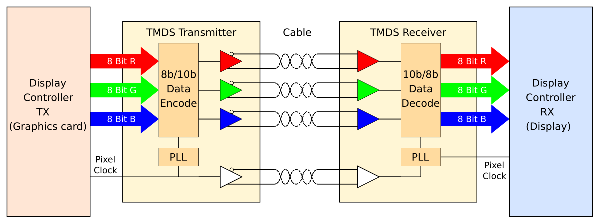
Announcement

Collapse
No announcement yet.

TMDSA/LTVMA...huh?

Collapse
X
 
  • Filter
  • Time
  • Show
Clear All
new posts

  • TMDSA/LTVMA...huh?

    TMDSA
    LTVMA

    Listed above are acronyms of sorts that I've noticed in the git repo for RadeonHD. Google turns up nothing, so does anyone know what they stand for? (Better yet, what they are for?)

    The only one I've pulled up is TMDS


    Rawr, thanks ^^

  • #2
    There are two digital output blocks in the 5xx and 6xx ASICs, which handle TMDS (the signalling for DVI and HDMI) and LVDS (the signalling for internal LCD panels). They sort of correspond to "digital output 1" and "digital output 2".

    The first block is TMDS only, and is called TMDSA (ie the first TMDS block).

    The second block can output TMDS or LVDS, and is called LVTMA (ie LVds plus TMds A or the first LVTM block).

    The two blocks are programmed differently. While we were preparing the initial documentation for 5xx and 6xx display logic we realized at the last minute that the information for the LVTMA block was missing from the documents. We were able to replace the 5xx document with a new one containing most of the 5xx LVTMA info but were only able to get the updated 6xx LVTMA info to Novell a few weeks ago. I'm hoping to get the same info posted publicly over the next week or two.

    As a result, until very recently if you had a card with dual DVI connectors there was a pretty good chance that one DVI connector (the one wired to the TMDSA block) worked and the other (the one wired to the LVTMA block) did not.

    Hope this helps.
    Test signature

    Comment


    • #3
      Thanks a bunch for the info ^^

      Comment

      Working...
      X